Gerber to Prototype
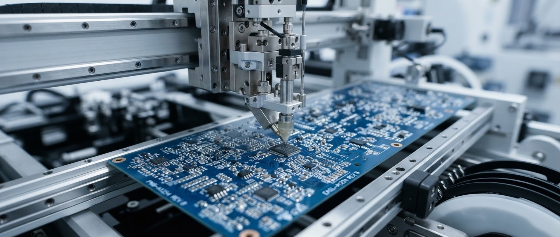
Upload Gerber-ready designs for rapid PCB fabrication and automated optical inspection, securing guaranteed corridor logistics and line capacity.
High-Yield Prototyping Capabilities
We combine automated digital parsing with physical line optimization to deliver functional prototypes that scale seamlessly.
Rapid Turnaround
Automated Inspection
Scale-Ready Path
Go from Gerber sign-off to physical assembly in one week with automated line scheduling.
Rigorous automated optical inspection ensures maximum first-pass yield on complex high-density boards.
Transition prototypes directly to audited volume production with full landed cost transparency across the India-ASEAN corridor.
Engineered to Exacting Standards
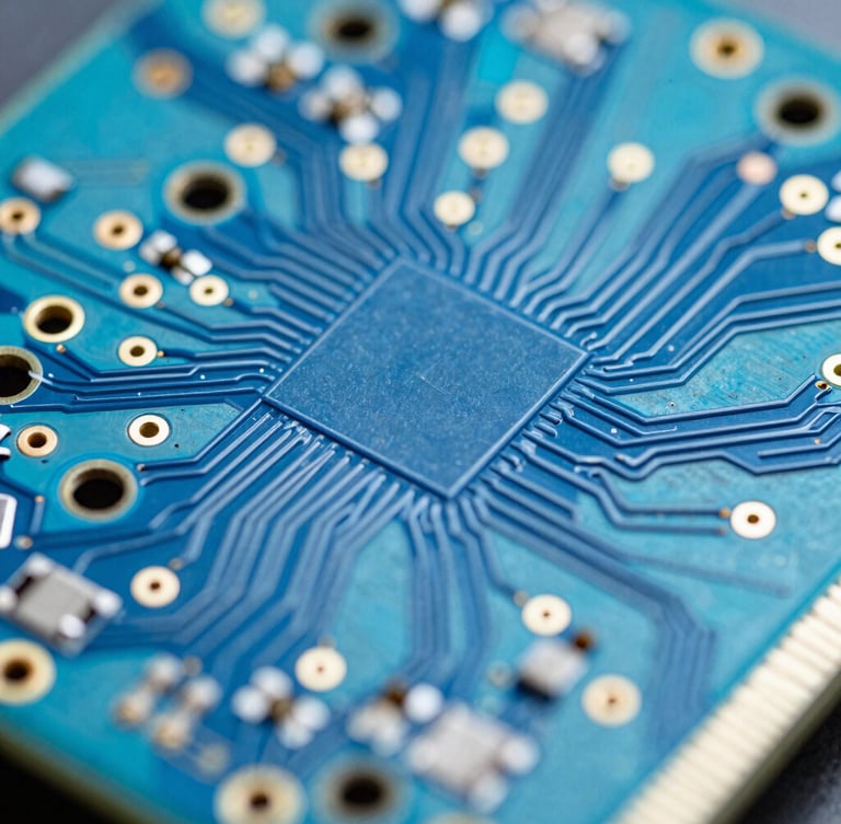
Our quick-turn lines support high-density interconnect designs with multi-region redundancy to secure your volume transition.
Min Trace / Space
3 mil / 3 mil (75 microns) for high-density routing.
Layer Count
1 to 32 layers with blind and buried microvias.
Surface Finishes
ENIG, HASL, OSP, and Immersion Silver options.
Component Pitch
Down to 0.35 mm for ultra-fine pitch BGAs.
Ready for Gerber Upload
Upload your design files now. Our AI engine parses your BOM and Gerber files to generate a multi-region quote in minutes.
INDOTHARA Electronics Solutions
Cross-border hardware supply chain orchestration.
Ecosystem
Home
RFQ
Services
Solutions
Corridor Offices
info@indothara.com
Chennai • Bangkok • Taipei • Shenzhen
ISO 9001:2015 Certified Operations
© 2026 INDOTHARA Electronics Solutions-Secure hardware supply chain orchestration.
CHINA - TAIWAN - THAILAND - INDIA CORRIDOR